Upcoming Events: Auto Vision Summit 2026 | Smart Factory Expo 2026 | Live Demos Available

Electronics Manufacturing

AI Vision for PCB & Electronics Manufacturing

Inspect solder joints, verify component placement, and ensure circuit integrity at microscopic precision.

Electronics manufacturing requires inspection at a scale and precision that human operators cannot sustain — from microscopic solder joints to densely packed SMT boards with hundreds of components. Orama deploys vision AI that catches solder defects, placement errors, and marking anomalies at full production speed, giving quality teams the confidence that every board leaving the line meets specification.

Explore No-Code Platform
AI-powered PCB and electronics inspection system

Built For Production

Tuned for real line conditions, traceability requirements, and fast operator decisions.

Industry Focus

Electronics Manufacturing

99.9%

Defect detection accuracy on PCB assemblies

0.01mm

Component placement verification precision

60%

Faster inspection than manual AOI review

<2 weeks

Typical pilot deployment timeline

Industry Challenge

Why this industry needs smarter vision

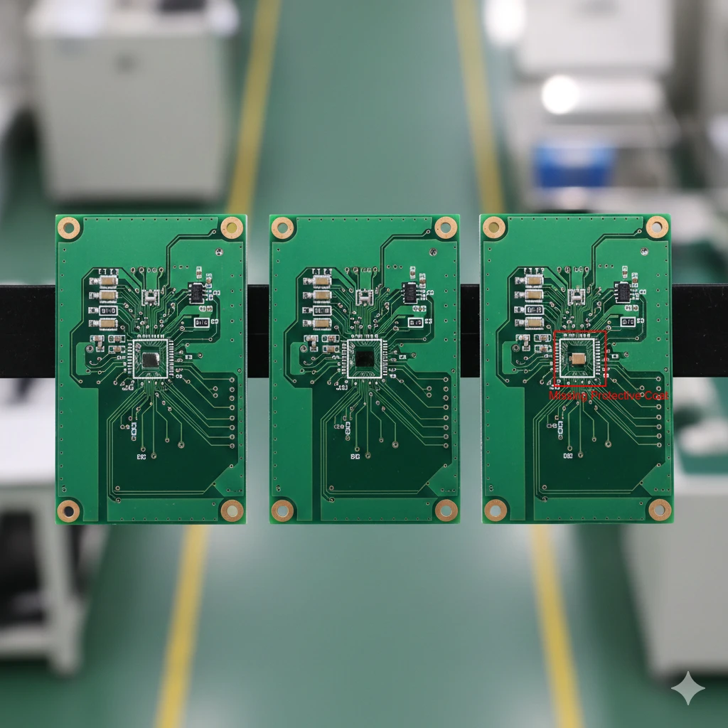
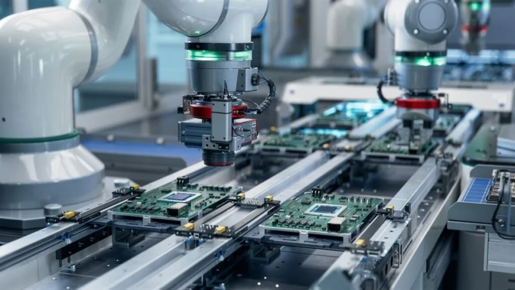
PCB and electronics inspection demands microscopic precision across hundreds of components per board, with defect types ranging from solder bridges and tombstoning to missing passives and wrong-polarity placements. Traditional AOI systems generate high false-positive rates, and manual review of flagged boards creates bottlenecks that slow production and increase the risk of real defects escaping to the field.

Solution Approach

How Orama addresses the challenge

Orama deploys deep learning vision models that inspect solder joints, verify component placement and orientation, read microscopic markings, and detect circuit trace defects with significantly lower false-positive rates than rule-based AOI. Each model is trained on your specific board designs and component libraries, so inspection accuracy improves with every production run.

Typical Project Flow

  • Imaging setup and data capture review
  • Model tuning around line variation
  • Pass or fail logic and deployment

Applications

How Orama applies to this industry

PCB & Component Inspection

Detect solder bridge, tombstoning, missing components, and circuit anomalies on PCBs.

  • Identifies solder bridge and insufficient solder
  • Detects component misalignment (0.01mm accuracy)
  • Finds lifted pins and tombstoning effects
  • Checks for circuit trace defects

99.9% defect detection, 60% faster inspection

SMT Component Placement

Verify correct placement, orientation, and presence of SMT components on circuit boards.

  • Verifies component polarity and orientation
  • Checks for missing or misplaced components
  • Validates solder paste application
  • Ensures proper chip seating

100% placement accuracy, zero orientation errors

Micro-component Marking

Read microscopic serial numbers, lot codes, and component markings for traceability.

  • Reads laser-etched codes on chips (0.1mm size)
  • Verifies component authenticity markings
  • Cross-references with manufacturing database
  • Ensures proper date/lot coding

100% traceability, counterfeit prevention

Visual Comparison

Before & after Orama

Before
After
Slide

FAQ

Frequently Asked Questions

Next Step

Ready to explore how Orama fits your industry?

We can adapt the same platform for your product geometry, lighting, line speed, traceability rules, and reporting needs without forcing your team into a generic workflow.

View All Industries

Project Fit

  • Single station pilots or full multi-line rollouts
  • Camera, PLC, and edge hardware aligned to your plant setup
  • Traceability, dashboards, and pass or fail logic tailored to the line